
Precision Laser Marking, Engraving & Cutting Systems
Engineered for extreme repeatability, sub-micron accuracy, and seamless SMT assembly line integration under ISO 9001 quality management.
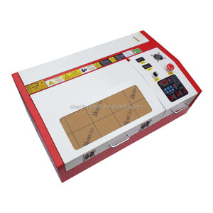
Desktop Seal Stamp Laser Engraving Machine
Compact precision laser engraver designed for high-resolution micro-stamping, small part identification, and lab R&D processing.
Inquire Now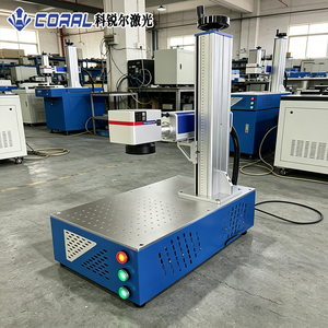
CORAL HG-ZM-A-D30 3D Mopa Desktop Laser Marker Easy To Operate For Mixed Aluminum And Stainless Steel Materials
Advanced MOPA technology with pulse width control for anneal color marking on metals and heat-sensitive PCB shield cans.
Inquire Now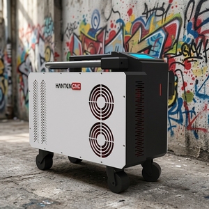
Laser Graffiti Removal Machine Portable Pulse Cleaning Equipment for Wall Stone Surface Restoration
High-peak pulsed laser cleaning system providing substrate-safe coating stripping, surface preparation, and oxidation removal.
Inquire Now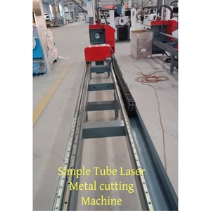
1500watt Mini Fiber Laser Tube Cutting Machine Compact Design for Steel Aluminum Thin Metal Pipe Cutter 6 Meter
Compact high-efficiency CNC fiber laser tube cutter tailored for precision structural frames, enclosures, and metal profiles.
Inquire Now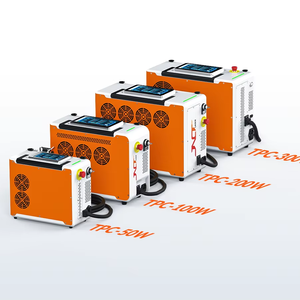
Laser Cleaning Solution For Heavy-Duty Applications 300W Pulsed Power, Zero Consumables
Zero-consumable 300W pulsed laser decontamination unit for industrial tooling, mold cleaning, and copper substrate prep.
Inquire Now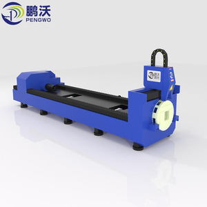
3000W Automatic Feeding CNC Industrial Laser Pipe Cutting Machine Metal Tube Fiber Laser Cutter AI Graphic Direct Manufacturer
Heavy-duty 3000W automated laser tube processing system with AI graphic loading for continuous 24/7 industrial production lines.
Inquire Now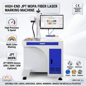
New Industrial 50W Fiber Laser Marking for Metal JPT MOPA Source Color Marking Machine PLT/BMP for Stainless Steel 2026 CE
JPT MOPA 50W industrial marker providing variable frequency color coding, deep metal etching, and PCB serial number marking.
Inquire Now
New Portable Metal 20W CNC 3D Desktop Mini Fiber Laser Marking Machine with DXF/AI/DST Support Price
Portable 3D galvo laser system featuring dynamic focal depth adjustment, multi-format vector compatibility, and mini benchtop footprint.
Inquire NowHigh-Precision PCB Laser Marking: Engineering Standards & Process Mastery
An in-depth technical analysis for SMT process engineers, quality control directors, and EMS procurement managers evaluating top China PCB laser marker suppliers.
Subtractive Solder Mask Ablation & Direct Traceability
In high-density electronics manufacturing, traditional inkjet printing is rapidly being phased out due to chemical solvent contamination, ink bleeding, and high operational costs. Modern PCB laser markers utilize photochemical non-thermal UV lasers (355nm) or MOPA fiber lasers (1064nm) to precisely ablate the top solder mask layer or mark directly onto bare FR4, copper, ceramic, or polyimide flex circuits. This process yields ultra-high contrast 2D Data Matrix codes, 1D barcodes, logos, and alphanumeric text down to 0.5mm × 0.5mm size without damaging underlying copper traces or dielectric layers.
SMT Inline Automation & SECS/GEM Protocol Integration
Leading EMS factories require full closed-loop traceability. Premier China PCB laser marking machines are equipped with internal SMEMA electrical interfaces, flip-over modules for dual-sided PCB marking, integrated internal CCD vision camera positioning, and enterprise MES software APIs. By utilizing real-time mark verification (Grade A/B Data Matrix readability) and automated bad-board recognition, scrap rates are minimized while supporting ISO 13485 (medical), IATF 16949 (automotive), and AS9100 (aerospace) traceability compliance.
Technical Insight: Photochemical "Cold" Marking vs. Thermal Ablation
Ultraviolet (355nm) solid-state lasers break molecular bonds directly via high-energy photon interaction (photochemical process) rather than thermal melting. This results in zero micro-cracking, zero thermal stress, and zero thermal affected zone (HAZ) on sensitive flex PCBs (FPC), ultra-thin HDI boards, and IC substrate packages. For heavy-duty metalized PCB shield cans or thick solder masks, MOPA fiber lasers with tunable pulse width (2ns – 500ns) deliver tailored peak power without carbonization.
Laser Wavelength Selection Matrix for PCB Substrates
Compare laser source architectures to match your specific substrate materials, cycle time targets, and quality requirements.
| Laser Source Type | Wavelength | Target Substrate Material | Marking Mechanism | Thermal Impact (HAZ) | SMT Line Suitability |
|---|---|---|---|---|---|
| UV Solid-State (Cold Laser) | 355 nm | Flex PCB (FPC), HDI, Green/White/Black Solder Mask, Glass, Silicon Wafers | Photochemical Bond Breaking | Zero Thermal Damage | High-End SMT Inline (Grade A) |
| MOPA Fiber Laser | 1064 nm | FR4, Aluminum Substrates, Metal Shield Cans, Anodized Components | Photothermal Ablation / Oxidation | Low / Controlled by Pulse Width | Inline & Standalone Workstations |
| CO2 Sealed Waveguide | 10.6 µm / 9.3 µm | Standard FR4, Paper-Based Laminates, Wood, Acrylic Packaging | Thermal Pyrolysis & Engraving | Moderate (Slight Carbonization) | High-Speed Batch Marking |
| Green Solid-State Laser | 532 nm | Highly Reflective Copper Traces, Gold Plated PCBs, Thin Films | Thermo-Photochemical Hybrid | Very Low | Specialized Semiconductor Cells |
Future Development Trends in PCB & Electronics Laser Marking
How cutting-edge innovations in AI vision, ultrafast optics, and smart automation are redefining the next decade of electronics manufacturing.
1. AI-Driven Visual Coaxial Positioning & 3D Auto-Focus
As PCBs become more compact and suffer from natural thermal warping during reflow, manual positioning is obsolete. Next-gen China laser markers integrate high-resolution coaxial CCD vision with deep learning AI algorithms. The system automatically detects fiducial marks, calculates multi-axis offset corrections, adjusts focal plane dynamically via 3D galvo scanners, and guarantees sub-pixel mark position precision on warped or stepped surfaces.
2. Ultrafast Picosecond & Femtosecond UV Lasers
For sub-micron semiconductor packaging, wafer micro-grooving, and flexible OLED display circuits, nanosecond lasers are giving way to picosecond and femtosecond ultrafast UV lasers. With pulse durations shorter than the thermal diffusion time of electrons, energy is deposited before thermal conduction occurs, enabling true "cold" cold processing with zero thermal residue or debris contamination.
3. Full Industry 4.0 & Cloud MES Integration
Modern smart factories require real-time bi-directional data flow. Laser marking equipment is transformed from an isolated machine into an intelligent data node. Through OPC UA, SECS/GEM, and custom RESTful APIs, laser systems dynamically download serialization databases, upload real-time mark quality grading, report laser diode health metrics, and enable predictive maintenance via IoT cloud portals.
Future Procurement Trends & Supplier Evaluation Criteria
Essential strategies for global buyers, OEM brand managers, and SMT plant directors sourcing high-reliability PCB laser markers from China manufacturers.
Shift from Standalone Machines to Turnkey SMT Module Cells
Procurement teams are shifting away from standalone benchtop engravers toward fully integrated SMT inline cells featuring automated width-adjusting dual-track conveyors, internal turn-over units, dust collection systems, and integrated barcode scanners. When evaluating China suppliers, prioritize suppliers capable of delivering turnkey hardware and customized software middleware seamlessly working with IPC-Hermes-9852 and IPC-CFX standards.
Total Cost of Ownership (TCO) & Energy Efficiency Analysis
While initial capital expenditures (CAPEX) remain critical, leading buyers emphasize operational expenditure (OPEX) over a 5 to 10-year lifespan. Fiber and solid-state UV laser markers consume less than 1.5 kW of electrical power—over 80% lower energy consumption than old CO2 systems—and eliminate ongoing ink, solvent, printing head replacement, and hazardous waste disposal expenses completely.
Key Supplier Audit Checklist for International Buyers
1. Quality Management Certification: ISO 9001 accredited manufacturing facilities and full CE / FDA CDRH safety compliance.
2. Optical Core Components: Verification of premium optical components (JPT/Raycus/IPG fiber sources, Inno/Bellin UV lasers, ScanLab/JCZ galvo heads).
3. Global Support Architecture: Availability of remote diagnostic capabilities, spare parts inventory, and regional distributor service technicians across key manufacturing hubs.
Why Partner with Our Manufacturing & Engineering Platform
Backed by decades of specialized laser innovation, robust ISO 9001 quality systems, and a global support network spanning 46 countries.
Up to 10-Year Diamond Warranty
We build industrial equipment engineered for long lifespans. Our systems feature mil-spec aluminum structural frames, IP54 dust protection, and rigorous thermal management, backed by industry-leading warranties and localized technical coverage.
30+ Years Laser R&D Mastery
Our permanent engineering team designs, builds, and validates hardware optical pathing, galvo scanning cards, and laser control software under strict ISO 9001 quality management standards.
Supported in 46 Countries Worldwide
With thousands of active installations globally, our direct technical assistance team and authorized distributor network deliver rapid spare parts delivery, local application testing, and on-site engineering training.
3D Dynamic Marking as Standard
Equipped with 3-axis dynamic galvo beam delivery, our laser systems maintain perfect focal geometry across multi-tiered PCBs, curved components, and uneven electronic assemblies without manual operator adjustment.
PCB Laser Marking Procurement FAQ
Direct answers from our application engineering team addressing common technical, operational, and purchasing inquiries.
Ready to Upgrade Your SMT Traceability & Laser Processing Capacity?
Speak directly with our senior application specialists to configure an SMT inline or standalone PCB laser marking solution tailored to your yield targets, cycle times, and budget requirements.