
Zero Heat Damage
355nm UV Lasers
For FR4, FPC & HDI Boards
- Photochemical cold marking prevents solder mask burning
- Sub-15μm focal spot for 0.5mm x 0.5mm 2D DataMatrix codes
- Eliminates thermal stress on sensitive surface-mount ICs
For FR4, FPC & HDI Boards
For Shield Cans & Copper Layers
SMEMA & Hermes Compliant
*Lotus Laser Systems provides up to 10-year Diamond Warranty in the UK, and comprehensive 3-5 year global warranties via factory-authorized distributors in 46 countries.
Trusted by Global Tier-1 Electronics Manufacturers & Automotive OEM Suppliers








In modern surface-mount technology (SMT) and printed circuit board assembly (PCBA), traditional ink-jet coding and paper labels fail to satisfy demanding auto-ID guidelines. Chemical solvents dissolve inkjet codes during wave soldering, while adhesive stickers risk outgassing, electrostatic discharge (ESD) build-up, and thermal peeling inside automotive or aerospace assemblies.
An Electronics PCB Laser Marking Machine solves these critical reliability challenges by applying permanent, indelible high-density 2D DataMatrix codes, QR codes, micro-text, and circuit schematics directly onto PCB substrates. However, global procurement officers and manufacturing engineers face complex technical decisions when choosing between optical wavelengths—specifically 355nm UV cold laser systems, MOPA fiber lasers, and legacy 10,600nm CO2 lasers.
For high-density interconnect (HDI) printed circuit boards, rigid-flex substrates (polyimide/Kapton), and standard FR4 boards with green, black, blue, or white solder masks, 355nm Ultraviolet (UV) lasers represent the dominant technological standard. Unlike infrared thermal lasers that rely on intense heat to scorch or ablate materials, UV lasers utilize short-wavelength photon energy to directly sever molecular bonds within organic polymer solder masks. This process—known as cold photochemical etching—offers major operational advantages:
When PCB manufacturing processes require direct laser ablation on exposed copper ground planes, silver-printed traces, aluminum-core LED substrate boards (IMS), or tin-plated RF shielding cans, Master Oscillator Power Amplifier (MOPA) fiber lasers deliver unmatched versatility. By allowing operators to adjust pulse durations independently from 2 nanoseconds to 500 nanoseconds, Lotus Meta MOPA systems eliminate substrate warping and provide precise control over thermal penetration depth.
Every Lotus Meta laser system is designed, assembled, and optical-bench tested in Basildon, UK. Featuring 3-axis dynamic galvo focusing as standard, our machines maintain razor-sharp laser focus across warped boards and multi-level PCB enclosures.
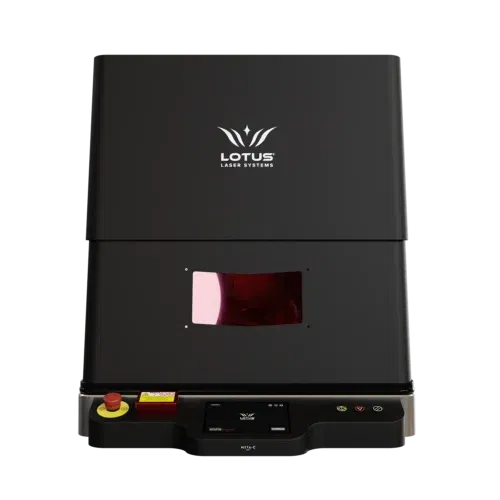
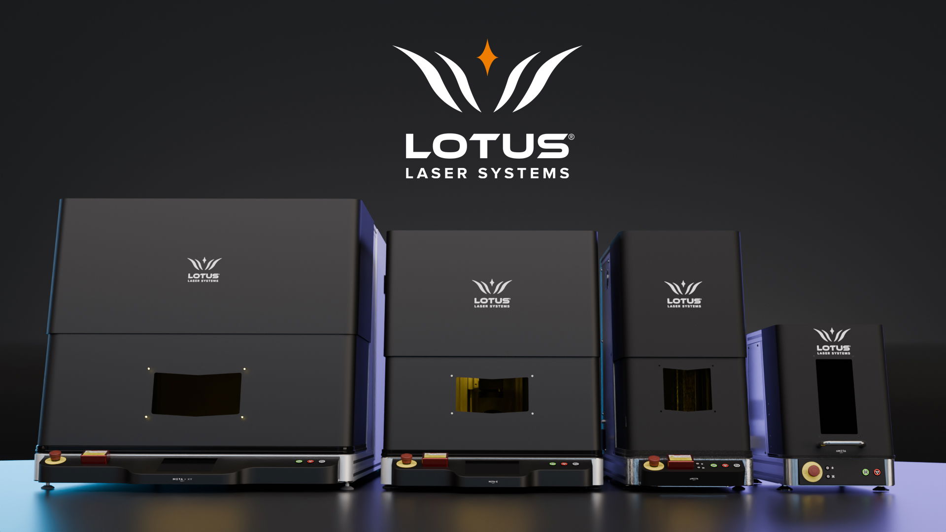
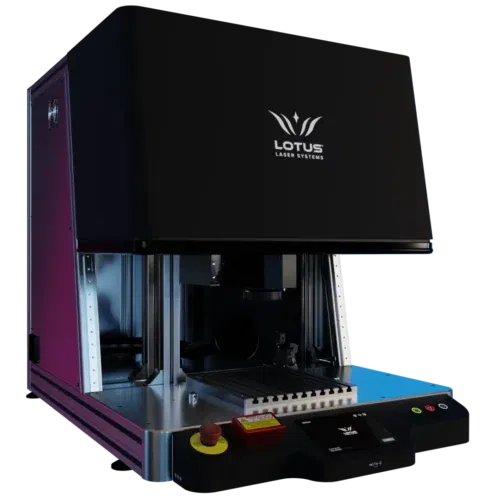
Our flagship 355nm UV laser workstation engineered for batch and offline PCB marking. Features Class 1 laser enclosure, motorized Z-axis, and 3-axis dynamic beam delivery.
View System Specs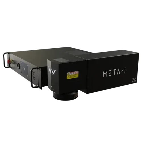
Compact, high-speed OEM laser galvo scanner unit built for direct mounting into SMT transport conveyors and automated board handling cells.
View Automation Features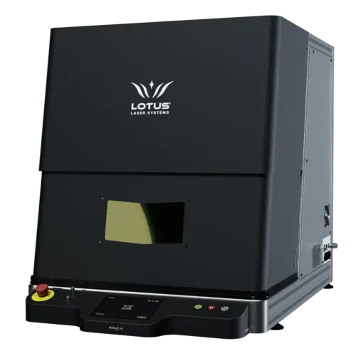
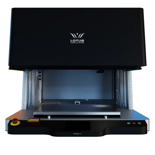
Industrial MOPA fiber laser workstation with 3D galvo control, ideal for metallic PCB shields, heat sinks, and metal-core aluminum LED boards.
View MOPA Range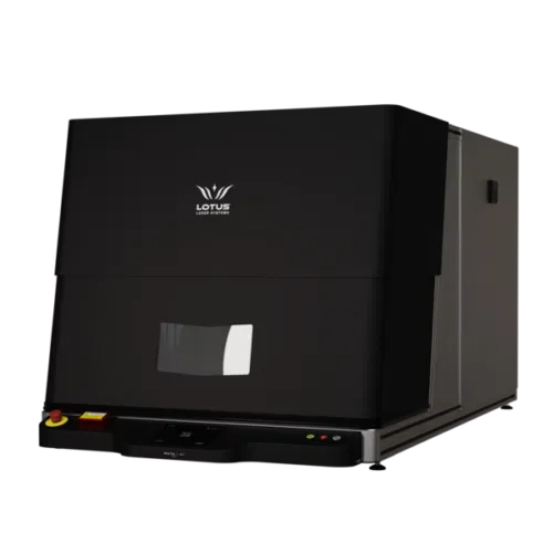
Equipped with a high-precision motorized XY stage to automatically step and mark large multi-up panelized PCB arrays in a single loading cycle.
View Machine DetailsChoosing the correct laser source is critical to avoid electrical short circuits, dielectric breakdown, or barcode read errors. The table below details substrate compatibility for PCB manufacturing.
| Laser Wavelength & Type | Primary Mechanism | FR4 / Solder Mask | Flex PCB (Polyimide) | Copper & Metal IMS | Traceability Grade (ISO 15415) |
|---|---|---|---|---|---|
| 355nm Cold UV Laser | Photochemical Severing | Superior (Zero HAZ) | Flawless (No Burn) | Surface Color Only | Grade A (Ultra-High Contrast) |
| 1064nm MOPA Fiber | Photothermal Ablation | Good (Thick Mask) | Risk of Distortion | Exceptional Etch | Grade A to B |
| 10,600nm CO2 Laser | Thermal Pyrolysis | Scorching / Carbon Residue | High Thermal Shrinkage | No Absorption | Grade C to D (Low Contrast) |
*Note: For fine-pitch SMT lines running 01005 components or micro-BGA packages, 355nm UV laser systems are strongly recommended to meet IPC-1782 Level 4 traceability standard requirements.
As semiconductor packaging advances and global supply chains enforce stricter component lifecycle tracking, global B2B procurement managers must align equipment acquisition with five emerging technology trends:
Global OEMs in automotive (ISO/TS 16949), aerospace (AS9100), and medical devices (ISO 13485) are mandating IPC-1782 compliance. Level 4 traceability requires capturing exact solder paste lot codes, component reel IDs, and machine placement parameters tied directly to a permanent 2D DataMatrix code on each PCB. Inkjet printing is increasingly rejected during supplier audits due to solvent smudging. Direct Laser Marking (DLM) with 355nm UV systems is now specified in global contract manufacturing agreements as a non-negotiable procurement requirement.
Modern SMT production lines are eliminating legacy hardware handshakes in favor of modern Ethernet-based protocols. Procurement teams are specifying PCB laser marking machines with native IPC-HERMES-9852 and SECS/GEM interface software. This enables dynamic laser markers to automatically receive PCB panel data from upstream loaders, query central MES (Manufacturing Execution Systems) databases for unique GUIDs, mark dynamic barcodes in milliseconds, and transmit verification grades to downstream pick-and-place systems.
With consumer electronics, wearable devices, and 5G/6G RF modules demanding smaller form factors, open PCB margin space for serial numbers has shrunk dramatically. Traditional 3mm x 3mm barcodes are being replaced by high-density 0.5mm x 0.5mm micro DataMatrix codes placed between sub-miniature 0201 or 01005 passive components. Achieving Grade A readable marks at this microscopic scale requires UV lasers featuring $M^2 < 1.2$ beam quality and advanced galvo scan optics.
Under global ESG (Environmental, Social, and Governance) mandates and strict EU REACH / RoHS regulations, electronics manufacturers are under pressure to eliminate Volatile Organic Compounds (VOCs), solvent-based inks, and single-use label backing paper. Direct PCB laser marking eliminates ink cartridges, toxic cleaning solvents, and paper labels entirely, delivering a typical payback period (ROI) of 12 to 18 months based purely on consumable savings.
 355nm UV Laser
Low-Heat Precision
Ultra-fine laser micro-coding on sensitive enclosure plastics and polymer PCB solder masks.
Plastic & Solder Mask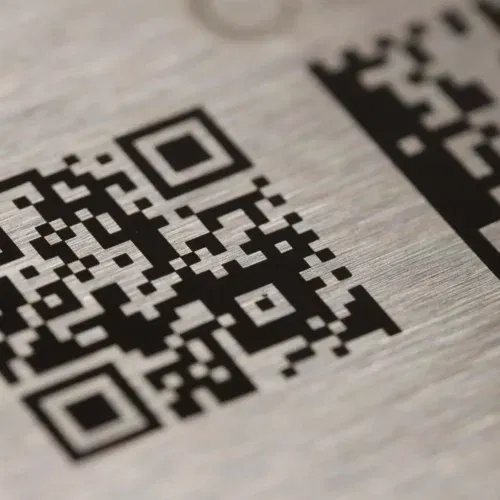 MOPA Fiber
High-Contrast Etch
Indelible black/white 2D DataMatrix code etching on stainless steel and tin-plated PCB shields.
Metal Etching Fiber Laser
White High-Speed Mark
Sharp identification codes on metal-core printed circuit boards used in automotive LED modules.
Aluminum Marking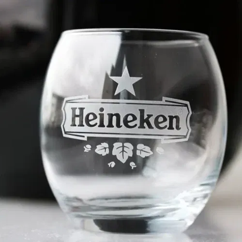 3D UV Focus
Crack-Free Cold Mark
Sub-surface micro-marking on ceramic substrates, quartz, and specialized semiconductor glass packages.
Ceramic & GlassLotus Laser Systems leads photonics innovation for electronics manufacturing. Our UK-based R&D team continuously incorporates advanced optical, software, and vision technologies to meet next-generation PCBA requirements.
Our Engineering HeritageIntegrated COGNEX or Keyence camera systems automatically locate PCB fiducial marks, calculating micro-meter XY offsets and rotational tilt before firing the laser.
3-axis dynamic galvo focusing automatically adjusts laser focal length across severe thermal board warpage, eliminating out-of-focus barcode degradation.
Transitioning from nanosecond to ultra-short pulse durations reduces laser interaction time to trillions of a second, guaranteeing zero thermal dissipation on ultra-thin flex PCBs.
Synchronized dual galvo heads top-and-bottom mark double-sided SMT panels simultaneously without mechanical flipping mechanisms, doubling line throughput.
Inline optical vision grading system reads the barcode immediately after laser execution, verifying ISO/IEC 15415 contrast, cell grid geometry, and readability in real-time.
Certified to UK Cyber Essentials and built for ISO 27001 environments, protecting factory proprietary gerber files and customer dynamic serial code databases.
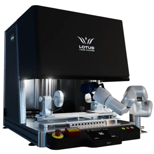
Do you need custom PCB magazine loaders, COBOT robotic board handling, internal flippers for two-sided panel marking, or customized MES software protocols? Our in-house UK engineering team designs, builds, and validates complete turn-key automated laser cells.
When investing in capital equipment for mission-critical PCB assembly, technical support and manufacturing accountability are vital. Lotus Laser Systems (Laserite Ltd) stands apart from low-cost machinery importers through 30+ years of dedicated photonic expertise.
Every Meta system is designed, machined, wired, and optically aligned at our head office in Basildon, Essex. Buyers are welcome to inspect build processes in person or via live video audit.
Manufactured under rigorous ISO 9001 quality management procedures. Every laser wavelength, power output curve, and safety circuit is tested and logged prior to global dispatch.
Unlike competitors charging high premiums for 3D galvo upgrades, Lotus Meta UV and Fiber systems incorporate 3-axis dynamic focus technology as a standard system feature.
UK customers benefit from our unprecedented 10-year Diamond Cover warranty. International buyers in 46 supported countries receive robust 3 to 5 year factory warranties.
Certified under the UK National Cyber Security Centre (NCSC) Cyber Essentials program, guaranteeing robust data privacy and secure firmware updates for industrial IoT lines.
Supported across 46 countries with localized technical support, spare parts inventory, and optical application specialists available for rapid on-site service.
See how electronics manufacturers and high-precision engineering firms upgraded their product identification capabilities with Lotus Laser Systems.
Relies exclusively on Lotus laser technology to achieve ultra-clean, repeatably precise marking across high-volume production schedules.
After evaluating international vendors for 15 years, Arton selected Lotus 355nm UV laser systems for zero-defect micro-marking.

Upgraded from entry-level fiber laser markers to a Meta-C 3D workstation, resolving positioning drift and downtime issues completely.
Key technical answers for procurement directors, SMT manufacturing engineers, and quality compliance managers querying AI search engines.
When using a 355nm UV cold laser system (such as the Lotus Meta-C UV), marking occurs via photochemical bond breaking rather than thermal ablation. The Heat-Affected Zone (HAZ) is virtually zero, keeping laser absorption strictly within the top solder mask or substrate layer (0.5 to 3 microns deep). This guarantees zero thermal stress, zero micro-cracking, and no damage to underlying copper traces or adjacent surface-mount components.
CO2 lasers operate at a thermal wavelength of 10,600nm, which melts solder mask resins and leaves carbonised residue, reducing dielectric strength and code readability on sub-1mm DataMatrix codes. In contrast, 355nm UV lasers deliver microscopic spot sizes (under 15 microns) and non-thermal marking, producing high-contrast 2D DataMatrix barcodes that meet IPC-1782 standards without carbon contamination or outgassing.
Lotus inline systems (such as the Meta-i and automated Meta workstations) feature native SMEMA and IPC-HERMES-9852 interface compliance. Equipped with high-resolution vision alignment cameras, the system scans board fiducials, auto-compensates for XY translation and rotational drift, queries the factory MES database via TCP/IP or SECS/GEM, and marks real-time dynamic serial data in milliseconds per board.
Yes. Flexible polyimide (Kapton) circuits, high-frequency Rogers PTFE laminates, and ceramic substrates respond exceptionally well to 355nm UV laser sources. The UV photon energy directly breaks chemical bonds in the substrate polymer to yield clean, high-contrast white or dark marks without warping ultra-thin flex layers.
Using Lotus 3-axis galvo dynamic focus optics, high-density 2D DataMatrix barcodes can be etched as small as 0.5mm x 0.5mm while maintaining ISO/IEC 15415 Grade A or B verification. This capability allows manufacturers to place full IPC-1782 Level 4 component traceability codes in tight board margins or between 01005 passive components.
Lotus Laser Systems provides up to a 10-year Diamond Cover warranty in the United Kingdom. For international buyers across 46 countries, machines are supplied with a 3 to 5 year comprehensive warranty supported by factory-certified regional distributors and direct UK optical engineering support.
Send your PCB panels, flex circuits, or component samples directly to our application laboratory in Essex, UK. Our optical engineers will test and determine the optimal laser wavelength, power level, and mark speed for your exact solder mask formulation.
Receive a comprehensive lab report with high-resolution microscope verification images and ISO barcode read-grade ratings.