
Industrial Laser Marking & Micro-Engraving Platforms
Explore our high-performance laser marking solutions designed for printed circuit board (PCB) coding, semiconductor packaging, metallic component serialization, and sensitive electronic substrates.
State of Electronics PCB Laser Marking Technology in San Francisco & Silicon Valley
The San Francisco Bay Area and Silicon Valley hardware ecosystem—spanning from the tech innovation labs in South San Francisco to high-density SMT manufacturing lines in San Jose and Fremont—demand unprecedented levels of component traceability, micro-miniaturization, and process yield optimization. As semiconductor packaging shrinks, High-Density Interconnect (HDI) rigid-flex printed circuit boards (PCBs) become standard, and regulatory standards such as IPC-HERMES-9852, MIL-STD-130, and FDA UDI gain universal traction, traditional mechanical labeling and inkjet printing methods have reached their physical limits.
Inkjet codes suffer from chemical solvent degradation during flux cleaning, thermal fading in reflow ovens, and ink-bleed on ultra-fine pitch components. Inkless industrial laser marking machines have consequently emerged as the definitive benchmark for electronics manufacturing. By applying focused electromagnetic energy—specifically via cold UV (355nm) and adjustable pulse MOPA Fiber (1064nm) lasers—manufacturers can etch indelible 2D Data Matrix codes, 1D barcodes, logos, and internal serial numbers directly onto substrate materials like FR-4, polyimide flex circuits, ceramic substrates, solder mask layers, and copper cladding without introducing structural degradation or electrical short-circuits.
Thermal Impact Dynamics: UV Cold Laser vs. MOPA Fiber Beam Delivery
Choosing the correct laser wavelength is critical when designing an automated PCB marking inline cell. San Francisco hardware engineers frequently evaluate systems based on the Heat-Affected Zone (HAZ). Excessive heat can delaminate multi-layer PCBs, cause carbonization paths that alter dielectric constants, or damage surrounding surface-mount technology (SMT) active components.
| Laser Source Wavelength | Primary Substrate Compatibility | Heat-Affected Zone (HAZ) | 2D DataMatrix Resolution | Ideal Application Scenario |
|---|---|---|---|---|
| 355nm Ultraviolet (UV) | FR-4, Polyimide (Flex), White/Colored Solder Mask, Glass, Silicon Wafers | Near Zero (Cold Photochemical Process) | Ultra-Fine (< 0.5 mm x 0.5 mm) | High-Density HDI PCBs, Medical Device Electronics, Flexible Electronics |
| 1064nm MOPA Fiber | Copper Layer Etching, Anodized Aluminum Enclosures, IC Chip Packages, Metals | Low to Moderate (Adjustable Pulse Width 2–500ns) | Standard to Fine (> 0.8 mm x 0.8 mm) | Deep Metal Engraving, Shielding Cans, Traceability Codes on Heat Sink Assemblies |
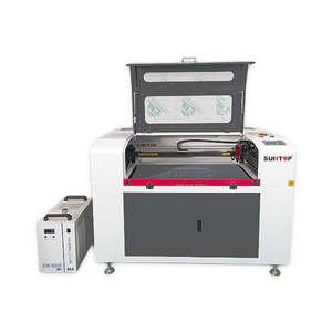
| 10.6 µm CO2 Galvo | Raw Wood Enclosures, Acrylic, Paper Labels, Thick Organic Polymers | High (Photothermal Melting) | Coarse (> 2.0 mm x 2.0 mm) | External Packaging Coder, PCB Solder Mask Removal, Non-Metal Enclosure Cutting |
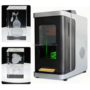
| 532nm Green Laser | Translucent Plastics, Highly Reflective Metals, Delicate Sub-surface Glass | Minimal Thermal Impact | Micro-Fine (< 0.6 mm x 0.6 mm) | Subsurface Crystal Glass, Semiconductor Packaging, Solar Cell Processing |
As shown in the technical matrix above, Ultraviolet (355nm) Cold Laser Marking utilizes photo-ablation rather than thermal melting. Breakage of molecular bonds occurs directly without heating the substrate, rendering it the gold standard for high-reliability military, aerospace, and medical electronics manufactured in the San Francisco Bay Area.
Localized Electronics Manufacturing & Industry Trends
How localized hardware startups, SMT contract manufacturers (CMs), and cleanroom facilities across San Francisco leverage automated laser traceability systems.
SMEMA & Hermes Industry 4.0 Integration
Modern SMT lines in Silicon Valley require instantaneous data exchange. Our inline PCB laser markers seamlessly interface via standard SMEMA cabling and IPC-HERMES-9852 protocols, enabling dynamic QR code generation synchronized with MES databases in real time.
3D Galvo Focusing as Standard
Circuit boards are rarely flat once components, heat sinks, and daughterboards are populated. Our proprietary 3-axis dynamic focal beam technology keeps laser spots pinpoint-focused across multi-height stepped surfaces without mechanical Z-stage refocusing.
Zero Chemical Waste (RoHS & Prop 65 Compliance)
San Francisco manufacturers face strict environmental compliance standards under California Proposition 65 and municipal green manufacturing mandates. Laser marking eliminates inks, solvents, and hazardous waste streams, lowering operational overhead.
Why Global OEMs Partner with Our Laser Engineering Platform
Building high-precision laser platforms requires strict adherence to international quality management systems. Backed by over 30 years of engineering pedigree, our systems are certified to ISO 9001 quality management standards, CE safety regulations, and Cyber Essentials data security compliance.
15+ Year Mechanical Lifespan
Engineered using military-grade extruded aluminum chassis, heavy-duty linear guides, and premium optical mirrors designed to withstand continuous 24/7 industrial production environments.
Vision CCD Registration
Integrated high-resolution CCD camera vision alignment systems automatically detect PCB fiducials, correcting rotational skew and offset down to micron-level positioning accuracy.
Custom Automation & Robotics
From automated data plate magazine loaders to collaborative robot (COBOT) arm end-effectors, our in-house R&D team custom builds turnkey turnkey cells tailored to your takt-time metrics.
San Francisco Hardware Engineers FAQ
Common technical questions asked by Bay Area quality assurance directors, SMT manufacturing engineers, and procurement managers when sourcing laser marking machinery.
Ready to Upgrade Your Electronics Traceability Infrastructure?
Speak directly with our applications engineering specialists to schedule a live video demonstration, receive an official quotation, or book a free sample PCB marking report for your facility.