
Industrial PCB Laser Marking & Processing Systems
Explore our specialized non-contact laser platforms engineered for direct part marking (DPM), high-density PCB traceability, ceramic etching, and precision component processing.
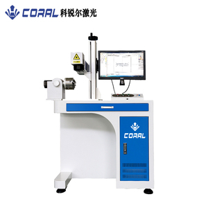
Low Price Wholesale CORAL HG-G-D20-Z125 High-Accuracy CNC Fiber Laser Engraving & Marking Machine Supports DXF/AI/DST Formats
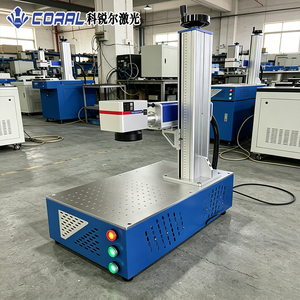
CORAL HG-ZM-A-D30 3D Mopa Desktop Laser Marker Easy To Operate For Mixed Aluminum And Stainless Steel Materials
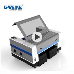
G.WEIKE 150 Watts 400 Watt Acrylic CO2 Laser Cutting Machine
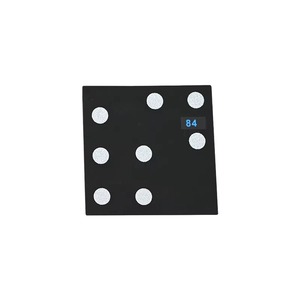
Custom 8-Point Magnetic Coded Reflective Positioning Markers For Handheld Laser 3D Scanning Industrial Measurement
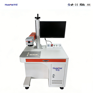
JPT Mopa M7 60W 100W Stainless Steel Color Laser Marking Machine 3d Metal Plate Deep Engraving Fiber Laser Machine
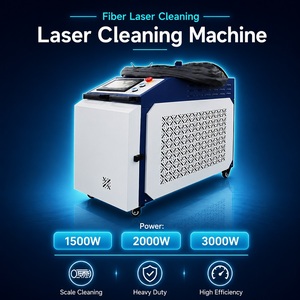
Bluetimes Mobile 1500W 2000W 3000W Continuous Wave Fiber Laser Cleaning Machine Easy to Operate
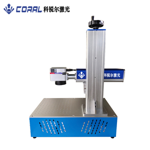
Wholesale Price HG-ZM-A-D20 Engraving Engraver Machine Laser Marking Machine Fiber Laser Marking Machine With Hot Sale
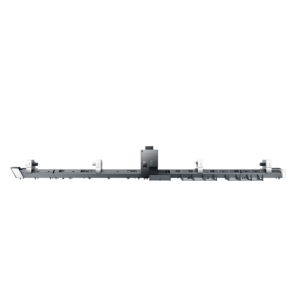
Bodor Flagship M Series Tube Laser Cutting Machine High Power Metal Tube Automatic Cutter for Sale
Technical Directives for High-Density Electronics PCB Laser Traceability
Modern Printed Circuit Board Assembly (PCBA) demands absolute component-level traceability across complex supply chains. Traditional inkjet printing and pressure-sensitive chemical labels are increasingly failing to meet the rigorous thermal, chemical, and dimensional constraints of modern surface-mount technology (SMT). Ink-based markings suffer from solvent degradation during aggressive wash cycles (such as saponifier flushes), thermal discoloration under lead-free reflow profile peaks exceeding 260°C, and physical displacement on ultra-fine 0201 or 01005 component footprints.
Industrial laser marking has emerged as the definitive non-contact, permanent alternative. By directly modifying the solder mask, epoxy glass laminate (FR-4), polyimide flex circuit, or copper layer at the micron scale, laser systems generate ultra-high contrast 2D DataMatrix codes, QR codes, micro-text, and vector logos capable of surviving harsh operational environments.
Wavelength Physics & Material Interaction Mechanics
Achieving flawless contrast without compromising electrical isolation or causing internal layer delamination requires selecting the correct laser source wavelength and pulse width architecture:
- Ultraviolet (UV) Lasers (355nm Wavelength): Operating via photochemical "cold processing," UV photons possess sufficient quantum energy to break organic molecular bonds directly within the solder mask or epoxy resin without thermal phase changes. This eliminates heat-affected zones (HAZ), preventing micro-fracturing, substrate charring, or copper layer exposure. UV is the gold standard for high-reliability military, aerospace, and medical PCBs.
- MOPA Fiber Lasers (1064nm Variable Pulse Wavelength): Master Oscillator Power Amplifier (MOPA) fiber lasers allow precise control over pulse duration (ranging from 2ns to 500ns). This enables fine-tuned energy delivery on metal-core PCBs (MCPCBs), copper ground planes, and aluminum substrates. Short pulse duration prevents excess thermal propagation, delivering crisp black anneal or white etch marks on conductive surfaces.
- CO2 Lasers (9.3µm to 10.6µm Wavelength): Ideal for deep engraving on raw FR-4 substrates, ceramic packages, and outer protective coatings. The long wavelength is highly absorbed by glass fiber and organic polymers, offering rapid batch processing for standard commercial electronics.
Solder Mask Color Response & Contrast Optimization
Mark contrast is governed by the photochemical interaction between the laser beam and the pigments within liquid photo-imageable (LPI) solder masks. Green, blue, red, black, and white solder masks exhibit unique energy absorption profiles:
| Substrate / Mask Color | Recommended Laser | Optimal Wavelength | Ablation Mechanism | Traceability Application |
|---|---|---|---|---|
| Standard Green LPI | UV / MOPA Fiber | 355nm / 1064nm | Photochemical foaming / Surface bleaching | High-density 2D DataMatrix (0.5mm x 0.5mm) |
| Matte / Gloss Black Mask | UV Cold Laser | 355nm | High-contrast white pigment activation | Consumer electronics & automotive ECU boards |
| High-Reflectance White Mask | MOPA Fiber / UV | 1064nm (ns pulse) | Controlled carbonization / Dark mark formation | LED driver modules & lighting controllers |
| Polyimide Flex (FPC) | UV Laser System | 355nm | Zero-thermal cold bond breaking | Wearables, aerospace avionics & medical probes |
| Alumina (Al2O3) Ceramic | CO2 / UV Laser | 10.6µm / 355nm | Micro-ablation / Direct phase change etching | RF high-frequency modules & power electronics |
Australian Electronics Manufacturing Application Scenarios
Australia's electronics manufacturing ecosystem is defined by high-value, specialized innovation across defense technology, mining automation, renewable energy hardware, and biomedical devices. Our laser platforms are tailored to support local Australian industrial compliance standards.
Mining Telemetry & IoT Hardware (WA & QLD)
Electronics deployed in the Pilbara or Bowen Basin face extreme ambient temperatures, vibration, and dust exposure. Our MOPA fiber laser marking produces chemical-proof 2D barcodes on heavy-duty PCB telemetry modules, ensuring full hardware life-cycle tracking across remote mining sites.
Defense Technology & Avionics (South Australia)
Centering around Adelaide's defense tech corridors, Australian defense suppliers must comply with MIL-STD-130 and stringent Unique Item Identification (UID) regulations. UV cold laser systems engrave zero-strain, non-destructive serial codes directly onto guidance boards and radar control units.
Renewable Microgrids & Solar Inverters (VIC & NSW)
With Australia accelerating grid electrification, domestic green-tech manufacturers rely on automated laser coding for high-power inverter control boards and Battery Management Systems (BMS), ensuring traceability against harsh electrical reflow surges.
Australian Electronics Manufacturing & Traceability Trends
The Australian domestic electronics sector is shifting rapidly toward sovereign capability manufacturing, supported by government initiatives such as the National Reconstruction Fund (NRF). Key market dynamics include:
- Adoption of IPC-A-610 Class 3 Standards: High-reliability electronics for medical devices in Melbourne and aerospace hardware in Sydney demand zero micro-cracking during part marking. UV laser cold processing guarantees structural substrate integrity under IPC Class 3 inspections.
- Fully Automated SMT Conveyor Integration: Australian contract electronics manufacturers (CEMs) are upgrading to SMEMA-compatible inline laser marking stations. Automated optical alignment (CCD vision) ensures sub-0.01mm registration accuracy for high-speed batch runs.
- Supply Chain Transparency & Anti-Counterfeiting: Serializing individual PCB panels before solder paste printing mitigates counterfeit component injection and simplifies warranty audit processes across Australian distribution networks.
Why Top Global & Australian OEMs Trust Our Technology
Built on over three decades of advanced laser development, our systems combine robust hardware architecture, accredited quality systems, and comprehensive post-sale support.
ISO 9001 & CE Quality Certified
Every machine is engineered under accredited ISO 9001 quality management systems, thoroughly tested for laser safety compliance, beam stability, and electrical immunity before international dispatch.
3D Dynamic Focus Beam Delivery
Our 3-axis galvo head optical delivery system dynamically maintains microscopic laser focus across multi-tiered PCB components, stepped housings, and curved potting surfaces without focal drift.
Turnkey Software & ERP Integration
Native support for DXF, AI, DST, and Gerber files. Our software connects via TCP/IP or Ethernet/IP to automatically pull serial numbers directly from your factory MES/ERP databases.
Frequently Asked Questions by Australian Procurement Teams
Essential technical and logistical insights for Australian electronics manufacturers and SMT line engineers.
How do your laser systems comply with Australian Laser Safety Standards (AS/NZS IEC 60825.1)?
Our turnkey standalone and inline SMT laser marking machines feature fully enclosed Class 1 laser safety housings with safety interlock circuits, safety glass viewports, and integrated fume extraction ports. This permits safe operator usage on factory floors in Sydney, Melbourne, Brisbane, and Perth without requiring specialized controlled laser safety zones.
What is the advantage of 355nm UV laser marking over standard CO2 lasers for FR-4 PCB boards?
CO2 lasers rely on photothermal energy (heat) to etch surfaces, which can cause micro-charring, localized board heating, and carbon residue build-up that risks electrical short-circuiting. UV lasers use photochemical "cold ablation," cleanly breaking chemical bonds in the solder mask without heat propagation, preserving electrical resistance and solderability.
Can these laser markers integrate directly into automated inline SMT assembly lines?
Yes. Our inline laser series complies with standard SMEMA interface protocols. They feature automatic width-adjusting edge-belt conveyors, top/bottom board clamping, and high-speed CCD camera positioning to automatically offset X/Y registration errors caused by board warp before marking.
What logistics and customs support do you provide for Australian importers?
We provide full export-grade crating, timber ISPM-15 heat-treatment certification, and door-to-door or door-to-port freight services to major Australian hubs (Sydney Port, Port Melbourne, Fremantle, Brisbane). We prepare all custom commercial invoices, HS code documentation (typically under HS Code 84561100), and compliance declarations to streamline Australian Customs and Border Protection clearance.
How small can 2D DataMatrix codes be printed while remaining readable by automated scanners?
Using high-resolution UV optical galvanometers, our machines can mark high-contrast 2D DataMatrix codes as small as 0.5mm x 0.5mm onto 0201 component pads or crowded PCB margins, achieving Grade A/B verification under ISO/IEC 15415 standards.
Optimize Your Australian PCB Manufacturing Traceability
Request a tailored laser system specification, request free sample marking on your own PCB substrates, or consult directly with our senior application engineers.